


Foldable display manufacturing yield challenges are real: many plants still report yields under 30%, far below the 60–70% seen in rigid OLED production.
That gap comes from stacking dozens of ultra-thin films into a sub‑1.0 mm sandwich that must bend at about a 1.5 mm radius.
A single particle, microcrack, or bad adhesive joint can turn a panel into scrap.
This post explains the main production defects—substrate fractures, contamination, misalignment, adhesive and hinge failures—and how each one drives scrap, testing time, and higher costs.
Core Yield Issues in Foldable Display Manufacturing
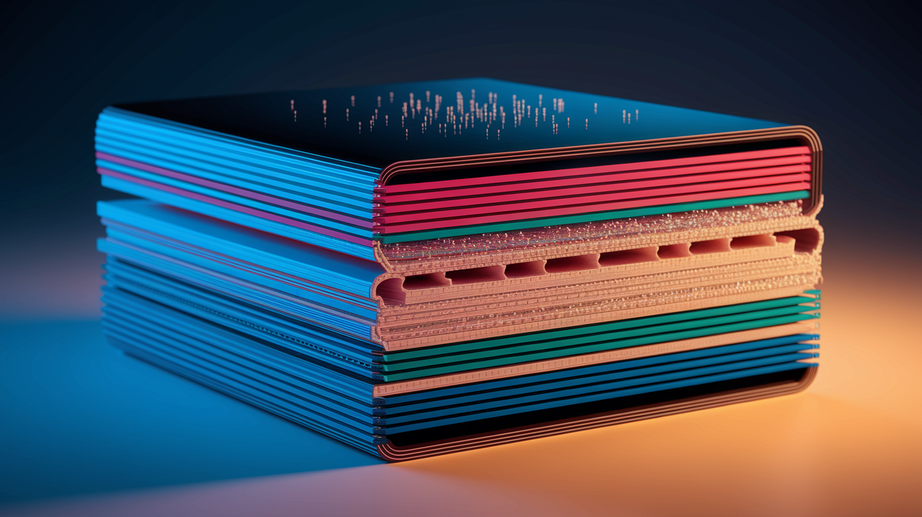
Making a foldable OLED display means stacking dozens of ultra-thin films into something under 1.0 mm thick. You’ve got polyimide substrates, flexible TFT backplanes, organic emitters, barrier coatings, touch sensors. Every layer adds steps, adhesive joints, alignment checks. Rigid smartphone screens use glass that stays dimensionally stable and forgives small mistakes. Flexible stacks don’t. They’re built on polyimide films and ultra-thin glass that bend, shift, react to temperature and humidity in ways that are hard to predict. So you get more ways for things to go wrong. Each new layer multiplies the chances of particles, chemical residues, or handling mistakes causing defects.
Right now, foldable display yields are under 30%. Compare that to the 60–70% you see in mature rigid OLED production for phones. The gap exists because foldable designs squeeze two really tough constraints at once: total thickness has to stay under 1.0 mm so the thing can actually flex, and the bend radius where it curves during folding needs to hit about 1.5 mm without cracking or peeling apart. Hitting both targets requires precision most factories are still figuring out. Lower yields mean more scrap, longer testing cycles, higher costs that hit everyone down the supply chain.
This yield problem hasn’t gone away across product generations because the fundamental technical barriers are still there. You’ve seen small improvements in UTG processing, better adhesive recipes, smarter hinge designs since 2019, but nothing has closed the gap to rigid-display performance. Samsung Display gets higher yields than most competitors thanks to years of experience and owning more of the supply chain, but even they’re stuck well below 60%. Until yields can consistently break 50%, foldable displays will cost more and stay limited to expensive flagship phones.
Six things killing yield in foldable display manufacturing:
- Substrate microcracks — Ultra-thin glass (30–100 µm) and polyimide films crack under handling stress, thermal cycling, or uneven adhesive curing. Some fail right away, others develop cracks later during fold tests.
- Particle contamination — Dust, fibers, chemical residues trapped between layers create visible defects, electrical shorts, or stress points that turn into delamination after bending a few times.
- Layer misalignment — Registration errors of just a few microns between TFT backplanes, emissive layers, and touch sensors cause pixel problems, uniformity issues, or broken traces at the fold line.
- Adhesive failures — The shear and peel forces from folding make adhesive layers creep, debond, or develop voids, especially at fold-zone interfaces where stress peaks.
- Hinge-induced stress — Mechanical hinges create tension and compression hotspots that push past material fatigue limits, triggering delamination or permanent creasing after thousands of cycles.
- Electrical discontinuities at the fold line — Flexible metal traces or ITO patterns crack or lift under repeated bending, breaking the circuits that control pixels or touch sensing.
Material Stack Challenges Behind Foldable Display Yield Loss
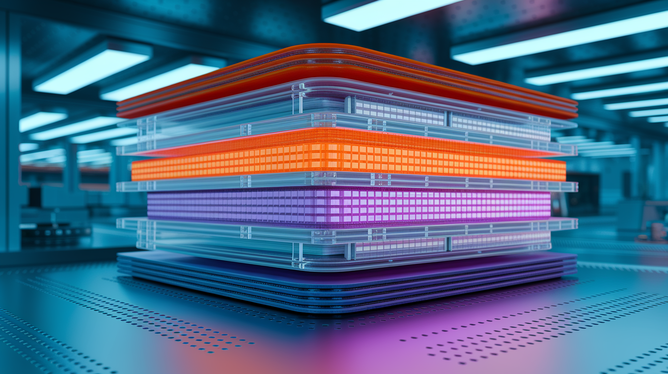
Ultra-thin glass in the 30–100 µm range resists scratches better than polymer films but it’s brittle. A tiny subsurface flaw can spread under repeated bending and cause total failure after just a few thousand folds. Polyimide substrates flex well but they’re super sensitive to particles. Even contamination smaller than a micron can punch pinholes that wreck barrier performance or create visible bright spots. The requirement to keep total stack thickness under 1.0 mm forces suppliers to thin every layer: OLED emitters, encapsulation barriers, cushion films, touch sensors. When you push materials into these extreme thickness ranges, defect rates go up fast. Colorless polyimide and hard-coat layers give you optical clarity and surface toughness, but they tend to crack or delaminate when bent to 1.5 mm radii. Multi-buffer cushion layers help spread stress away from brittle parts, but each film you add means another adhesive bond, another alignment step, another chance for contamination.
UTG develops mechanical fatigue as edge chipping during die separation or micro-fractures at fold-zone boundaries where curvature is steepest. PI substrates handle bending better but they have surface roughness issues and coefficient-of-thermal-expansion mismatch with the inorganic layers next to them. Hard-coat films deposited on CPI boost pencil-hardness ratings but reduce how much the material can stretch before breaking, so they crack under repeated flexing. Adhesives picked for high peel strength under static load often creep or develop voids under cyclic shear, and vacuum lamination cuts down bubbles but adds cycle time and equipment cost. The interaction between material choices and process conditions creates a really narrow zone of acceptable performance. Small changes in temperature, pressure, or layer thickness push defect rates past what you can afford.
Four material-layer failure mechanisms limiting foldable display yield:
- UTG fracture — Edge cracks from laser cutting or mechanical scoring spread into the active area under bending stress, causing immediate or delayed electrical shorts and optical defects.
- PI surface defects — Particle embedment, micro-wrinkles, or incomplete planarization during substrate prep create surface bumps that prevent clean deposition of the next layers, leading to pixel non-uniformity or delamination.
- Hard-coat cracking — High-modulus coatings deposited to hit 3H–5H pencil hardness crack under tension when bent below their critical radius, exposing softer underlayers to scratches and moisture.
- Delamination at interfaces — Stress concentration at bond lines between different materials (organic-inorganic, rigid-flexible) exceeds how strong the interface actually is after tens of thousands of folds, causing lift-off and display failure.
Mechanical Stress and Creasing Effects on Yield
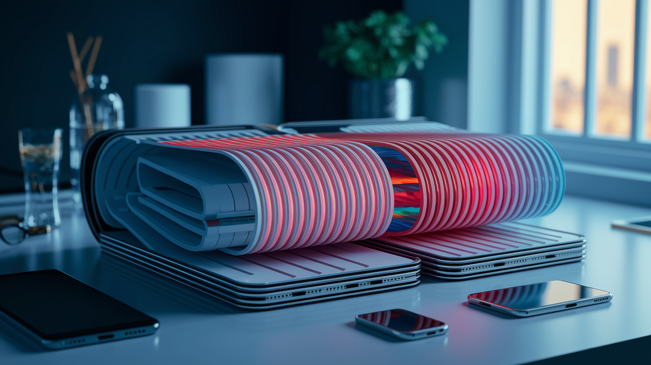
Foldable devices are designed to survive at least 200,000 fold cycles—roughly 100 folds a day for five or six years. Premium designs get validated to 400,000 cycles or more. Meeting those targets means controlling peak stress at the fold line, where tensile and compressive strains flip direction every time you open or close the device. Creases are permanent visible deformations along the fold axis, caused by plastic deformation in polyimide or adhesive layers that don’t bounce back to their original shape. Once a crease shows up, local stress concentration speeds up further deformation, creating a runaway problem. Hinge systems try to spread bending load across a wider arc, lowering peak curvature and reducing strain in the outer and inner layers. But they create new failure risks: hinge torque degradation, metal-on-metal wear debris, and misalignment of the display stack relative to the hinge axis.
In-fold designs (where the display bends inward to protect the screen) let you build thinner modules but they put compressive stress on the OLED stack and tensile stress on the backplane and substrate. This asymmetry makes in-fold configs harder to manufacture with good yield because the compressed side is more vulnerable to buckling and delamination, while the tensile side risks trace fractures in metal interconnects. Out-fold designs (display curves outward) reverse the stress profile and are generally easier to produce, but they expose the flexible OLED surface to impacts and scratches, so you need harder cover films that are inherently less flexible. Manufacturers are constantly trading thinness and user experience against manufacturability and yield. No single hinge geometry or folding direction fixes everything.
Stress concentration modeling shows that even minor deviations in hinge alignment or cushion-layer thickness create localized hotspots where strain exceeds what the material can handle over time. Multi-axis hinges with cam or geared linkages help spread curvature more evenly, but they add mechanical complexity, tighter assembly tolerances, and wear debris that can migrate into the display stack. Drop-hinge designs that open past 180 degrees reduce stress at full extension but require stiffer materials that resist bending, pushing module thickness above target. Accelerated bending fatigue tests often miss real-world failure modes because lab fixtures impose idealized symmetric loads, whereas actual users introduce torsion, off-axis bending, and impacts that speed up crease formation and delamination in ways standard cycling tests don’t catch.
Contamination and Cleanroom Control in Foldable Yield Performance

Particle contamination between ultra-thin layers creates visible defects—dark spots, bright spots, mura (non-uniformity)—and electrical shorts when conductive particles bridge adjacent electrodes. Foldable OLED stacks need cleaner fabrication environments than rigid displays because flexible barrier films are thinner and more permeable, offering less room for error when contamination punches pinholes. A single 5-micron fiber trapped between the polyimide substrate and the TFT backplane can lift the surrounding layers during lamination, creating a void that turns into delamination after a few hundred folds. Moisture getting in through defective encapsulation speeds up organic-material degradation, producing dark spots and brightness decay within weeks of field use. Moisture vapor transmission rate requirements for flexible barriers are typically below 10⁻⁶ g/m²/day, orders of magnitude tighter than rigid-display encapsulation targets. Hitting this spec across a bendable interface remains a persistent problem.
Cleanroom classification alone doesn’t guarantee low contamination. What matters is particulate control at critical steps: substrate cleaning before backplane deposition, pre-lamination surface prep, and final encapsulation sealing. Many fabs operating at ISO Class 5 (≤3,520 particles ≥0.5 µm per cubic meter) still see yield loss because handling equipment and tooling introduce localized contamination spikes during wafer transfer or vacuum break. Advanced barrier films using alternating inorganic-organic multilayers improve MVTR performance but they’re sensitive to pinholes from particles present during deposition. Even a single defect can compromise an entire module. The lack of perfect encapsulation under dynamic bending conditions increases field-failure rates, especially in humid or high-temperature environments where moisture diffusion accelerates.
| Contamination Source | Primary Impact on Yield |
|---|---|
| Airborne particles during lamination | Visible defects (bright/dark spots), delamination initiation, electrical shorts between layers |
| Moisture ingress through barrier defects | Organic material degradation, luminance decay, dark-spot growth, shortened product lifetime |
| Chemical residues from adhesives or solvents | Interfacial contamination reducing adhesion strength, outgassing causing voids, optical haze |
| Handling-induced fiber or skin-oil transfer | Localized layer lift-off, stress concentration leading to crease formation, touch-sensor malfunction |
Alignment Precision and TFT Backplane Issues in Foldable Displays
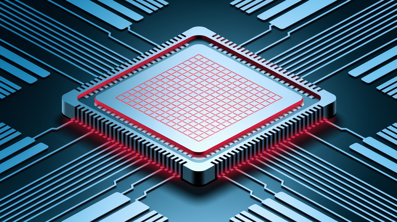
Flexible TFT backplanes—whether low-temperature polysilicon (LTPS) or indium-gallium-zinc oxide (IGZO)—need micron-level alignment across multiple photolithography and deposition steps to deliver pixel uniformity and electrical connectivity. When the substrate is a flexible polyimide film instead of rigid glass, dimensional stability becomes the limiting factor. Thermal expansion, humidity absorption, and mechanical tension during processing all shift layer registration. Misalignment of even 2–3 microns between the gate metal, source-drain metal, and passivation layers produces pixel defects—stuck-on pixels, stuck-off pixels, or brightness non-uniformity—that are immediately visible and can’t be repaired. At the fold line, where curvature is steepest and mechanical stress highest, even perfect initial alignment can drift as the substrate deforms under repeated bending.
IGZO TFTs offer better uniformity and lower leakage current than amorphous silicon, but IGZO thin films are sensitive to hydrogen and oxygen exposure during bending, which can shift threshold voltage and degrade switching performance. LTPS TFTs deliver higher electron mobility and faster pixel response but require laser annealing steps that introduce thermal stress gradients in flexible substrates, increasing the risk of warp or layer delamination. Both backplane technologies struggle with trace discontinuity at fold zones. Metal interconnects running perpendicular to the fold axis experience tension-compression cycling that starts fatigue cracks after tens of thousands of folds, eventually breaking circuits that control rows or columns of pixels.
Automated optical inspection systems scan completed backplanes for pixel anomalies, but catching latent defects—microcracks or adhesion weaknesses that only show up after fold cycling—requires destructive testing or time-consuming reliability qualification. Inline AOI catches obvious problems like missing pixels or short circuits, but it can’t predict which units will fail after 100,000 folds. Manufacturers have to over-sample early production lots for extended cycling tests, which lengthens time-to-market and raises the cost of yield learning.
Three pixel/line defect modes caused by alignment errors in flexible TFT backplanes:
- Pixel electrode misalignment — Anode or cathode contacts fail to overlap properly with TFT source/drain, creating high-resistance connections that produce dim or non-functional pixels.
- Via chain opens — Interlayer vias connecting metal layers shift out of registration, breaking electrical paths and causing entire rows or columns to fail.
- Passivation layer gaps — Misaligned dielectric layers expose metal traces to moisture or create unintended capacitive coupling between adjacent lines, leading to crosstalk or electrical shorts.
Adhesives, Lamination Defects, and Interlayer Reliability Impacting Yield

Adhesive layers in foldable displays have to bond different materials—polyimide to UTG, OLED stack to cushion film, touch sensor to cover window—while handling cyclic shear and peel forces that reverse direction with every fold. Optically clear adhesives picked for high transparency and low haze often creep under sustained load, letting layers shift or debond at fold lines where stress concentrates. Voids and bubbles form during lamination when trapped air, solvent outgassing, or particle contamination prevents complete adhesive wetting. Even sub-millimeter bubbles act as stress concentrators under bending, starting delamination that spreads outward with each fold cycle. Vacuum lamination cuts bubble formation by removing air before adhesive cure, but it adds process time and requires precise pressure control to avoid over-compressing fragile layers.
Adhesive bond-line thickness variation—often caused by uneven pressure distribution across large panels or substrate warpage—creates non-uniform stress fields that speed up fatigue failure. Thermally cured adhesives offer stronger final bonds but introduce thermal budget constraints that can degrade temperature-sensitive OLED materials or shift TFT electrical characteristics. UV-cured adhesives cure faster and at lower temperatures but often have lower peel strength and are more susceptible to moisture-induced degradation. The tradeoff between cure speed, bond strength, and process compatibility leaves a narrow window of acceptable adhesive performance, and small variations in supplier material batches can shift yields by several percentage points.
Five common lamination defect types in foldable display manufacturing:
- Void formation — Air pockets or outgassing bubbles trapped between adhesive layers that reduce bond area, create optical defects, and start delamination under bending stress.
- Edge delamination — Incomplete adhesive coverage or poor edge sealing allows moisture ingress and mechanical peel initiation at module perimeters, progressing inward over time.
- Adhesive squeeze-out — Excess adhesive extruded beyond bond lines contaminates adjacent surfaces, interferes with electrical contacts, or creates optical artifacts visible to end users.
- Newton ring interference — Insufficient or uneven adhesive thickness produces optical interference patterns (Newton rings) visible under ambient light, failing cosmetic quality standards.
- Particle-induced lift-off — Contaminant particles prevent full adhesive contact, creating localized high-stress zones that spread into larger delamination areas after cycling.
Testing, Quality Assurance, and Yield Measurement for Foldable Displays
First-pass yield (FPY)—the percentage of units passing all electrical, optical, and mechanical tests on the first try—is the main manufacturing metric. Foldable displays hit FPY well below 30% because multi-material stacks and moving hinge interfaces introduce defect modes you don’t see in rigid displays. Electrical testing checks pixel functionality, touch-sensor response, and TFT uniformity across the active area, but these static tests can’t predict fold-cycle reliability. Units that pass initial electrical inspection often fail during accelerated lifetime testing, when 200,000 to 400,000 simulated folds reveal latent adhesive failures, hinge wear, or trace discontinuities.
Electroluminescence mapping captures pixel brightness and color uniformity before and after fold cycling, catching degradation invisible to pass/fail electrical tests. Nano-indentation measures local hardness and elastic modulus of cover films and hard coats, correlating mechanical properties with scratch resistance and crease susceptibility. Adhesion testing—lap-shear, 90-degree peel, and cyclic fatigue—quantifies bond strength under conditions simulating real-world folding. Highly accelerated life testing (HALT) and highly accelerated stress screening (HASS) protocols subject units to combined thermal cycling, humidity, vibration, and mechanical bending to discover early-life failure modes that escape standard qualification. But the lack of standardized durability pass criteria across the industry complicates quality acceptance. One manufacturer may validate to 200,000 cycles at 23°C and 50% RH, while another uses 400,000 cycles at 60°C and 85% RH, making yield and reliability comparisons difficult.
Long-duration fold-cycle testing creates a significant bottleneck. A single 200,000-cycle test at 1 Hz (one fold per second) takes over 55 hours per unit, and testing statistically significant sample sizes from every production lot delays shipment and ties up capital in test equipment. Failure analysis workflows rely on cross-sectioning, scanning electron microscopy, and atomic force microscopy to identify root causes of delamination, cracking, or electrical opens. But destructive FA consumes units that could otherwise be reworked or sold, further reducing effective yield. Inline inspection using automated optical inspection and electroluminescence cameras catches obvious defects—missing pixels, brightness non-uniformity, visible particles—but can’t detect subsurface adhesive voids or incipient microcracks that only become yield losses after fold testing.
Four commonly used QC and failure-analysis methods in foldable display production:
- Electroluminescence mapping — Captures spatial distribution of pixel brightness and color before/after cycling to detect degradation patterns and localize failure zones.
- Nano-indentation and pencil hardness — Measures mechanical properties of cover films and hard coats to predict scratch resistance and crease formation under bending.
- Cross-sectional SEM and AFM — Provides high-resolution imaging of layer interfaces, adhesive bond lines, and microcrack propagation to guide root-cause analysis of delamination and fracture.
- Cyclic adhesion fatigue testing — Applies repeated peel or shear loads to adhesive joints under controlled temperature and humidity, simulating real-world fold stresses and identifying weak formulations or process conditions.
Cost Impact of Low Foldable Display Yield

A rigid 7.3-inch QHD OLED module costs about $50, split between $35 for the display panel and $15 for the touch module. An equivalent foldable 7.3-inch WQHD OLED module costs around $100—$70 for the display and $25 for touch—doubling the component cost. This doubling reflects higher material costs (UTG, polyimide, specialized adhesives, advanced barrier films) and the direct impact of sub-30% manufacturing yields. When fewer than three out of ten units pass first-time quality checks, scrap and rework costs pile up, and usable inventory has to absorb the expense of all those discarded defective units.
Touch modules in foldable displays cost significantly more because they can’t use conventional rigid indium-tin-oxide patterns on glass. Metal-mesh and silver-nanowire sensors offer flexibility but require expensive patterning and encapsulation to prevent oxidation and maintain transparency. Samsung’s proprietary Y-Octa technology integrates touch sensing directly into the OLED stack, eliminating a separate touch film and cutting total cost. But it’s a competitive advantage limited to Samsung’s internal supply chain. For other display makers, touch-module cost remains a major driver of overall module expense, and low yields in touch-sensor lamination or patterning add another layer of scrap cost.
Supply-chain variability in raw materials—batch-to-batch differences in adhesive viscosity, polyimide surface roughness, or UTG edge quality—introduces unpredictable yield swings. Incoming quality assurance for critical materials requires statistical sampling and performance testing, but even rigorous IQA can’t catch every out-of-spec batch before it enters production, leading to yield excursions discovered only after expensive downstream processing. Suppliers with tighter process controls and longer production histories (such as established polyimide film producers or precision glass suppliers) command premium pricing, further raising material costs.
| Cost Driver | Effect on Production Cost |
|---|---|
| Sub-30% first-pass yield | Usable units must absorb costs of 70% scrap and rework, effectively tripling per-unit overhead and material expense |
| Specialized materials (UTG, metal-mesh touch, advanced barriers) | Raw material cost 1.5–2× higher than rigid-display equivalents; tight supplier base limits negotiation leverage |
| Extended qualification and reliability testing | Long-duration fold-cycle tests tie up capital equipment and delay revenue recognition; FA consumes units that cannot be sold |
Process Control, Automation, and Yield Improvement Strategies

Statistical process control frameworks monitor key parameters—adhesive dispense volume, lamination pressure, curing temperature, substrate cleanliness—in real time, triggering alerts when measurements drift outside control limits before defects accumulate. Root cause analysis workflows systematically trace yield excursions back to specific materials, equipment, or operator actions, enabling corrective action and preventing recurrence. Implementing SPC and RCA requires significant upfront investment in sensor instrumentation, data infrastructure, and cross-functional teams, but the payoff is a measurable reduction in process variability and a corresponding lift in yield.
Automation reduces human handling, which is a major source of contamination and mechanical damage. Robotic pick-and-place systems transfer flexible substrates without inducing stress concentrations or introducing particles from gloves or tools. Automated adhesive dispensing ensures consistent bond-line thickness and eliminates voids caused by manual application errors. Vision-guided alignment systems achieve micron-level registration between layers, compensating for substrate dimensional changes caused by temperature or humidity. Automation adds capital expense and requires regular calibration and maintenance. Smaller suppliers or new entrants often lack the scale to justify these investments, leaving them at a persistent yield disadvantage relative to vertically integrated industry leaders.
Design-for-manufacturability principles guide product architects to make choices that ease fabrication and improve yield: wider process windows for temperature and pressure, gentler bend radii that reduce peak stress, and material selections that tolerate greater thickness or alignment variation. Continuous improvement programs—Kaizen, Six Sigma, Lean Manufacturing—institutionalize incremental yield gains by empowering line operators to identify and fix small issues before they escalate. Supplier development initiatives work with raw-material vendors to tighten incoming specifications and improve batch-to-batch consistency, lowering the probability of yield-killing material defects.
Five yield-improvement tools and approaches in foldable display manufacturing:
- Real-time SPC dashboards — Monitor critical process parameters continuously and flag deviations before defects accumulate, enabling immediate corrective action.
- Automated substrate handling — Robotic transfer and alignment systems reduce particle contamination and mechanical stress from manual handling.
- Design-for-manufacturability reviews — Early-stage product design adjustments (bend radius, material selection, layer count) that widen process tolerances and reduce defect sensitivity.
- Supplier qualification and development programs — Work with raw-material vendors to tighten specs, improve batch consistency, and implement joint RCA on yield excursions.
- Accelerated learning cycles using HALT/HASS — Rapidly discover failure modes and stress limits through combined environmental and mechanical testing, feeding insights back into process adjustments.
Benchmarking Foldable vs Traditional Display Yield and Reliability
Traditional rigid OLED displays for smartphones hit manufacturing yields in the 60–70% range after process maturity, backed by decades of learning in glass handling, TFT lithography, and OLED encapsulation. Foldable OLED yields stay below 30%, even for third and fourth generation products, because the core technical challenges—ultra-thin substrates, extreme bend radii, multi-material adhesive stacks, and hinge-induced stress—haven’t been solved at scale. Samsung Display, thanks to vertical integration and years of pilot-line experience, reportedly gets yields modestly higher than competitors. But even industry leaders haven’t closed the gap to 50%.
Durability targets for foldable devices specify minimum fold-cycle lifetimes above 200,000 cycles, with premium models validated to 400,000 cycles or more. Rigid displays have no equivalent mechanical-cycling requirement. Their reliability focuses on drop resistance, thermal stability, and OLED lifetime (typically 50,000–100,000 hours to half brightness). This fundamental difference means foldable displays face an entirely new dimension of qualification testing, and no amount of rigid-display process maturity directly transfers to solving flexible-display yield challenges.
Cost deltas remain large. Foldable modules cost roughly double the price of equivalent rigid modules, driven both by material premiums and by the yield penalty. As yields improve from 30% toward 50%, per-unit costs will decline. But achieving 60–70% yields comparable to rigid OLEDs may require another generation of materials innovation, hinge redesign, and process automation. Until then, foldable displays will stay confined to flagship devices where premium pricing can absorb the cost burden.
Three comparative metrics: foldable vs. rigid OLED displays:
- Manufacturing yield — Foldable: <30% first-pass yield; Rigid: 60–70% first-pass yield. Gap driven by added process complexity, ultra-thin substrates, and cyclic mechanical stress.
- Cost delta — Foldable 7.3″ module: ~$100 (display $70 + touch $25); Rigid 7.3″ module: ~$50 (display $35 + touch $15). Doubling reflects material premiums and yield losses.
- Durability targets — Foldable: >200,000 fold cycles (premium >400,000); Rigid: no mechanical cycling requirement, focus on drop/shock and OLED lifetime (50,000–100,000 hours).
Final Words
In the action, we explained why yield stays low: ultra-thin stacks, fragile UTG/PI layers, hinge and creasing stress, particle contamination, alignment precision, and lamination failures raise defect risk and testing burden.
That gap — under 30% vs 60–70% for rigid OLEDs — increases costs and supplier pressure, but stronger process control, automation, and focused QA can raise first-pass yields.
Bottom line: foldable display manufacturing yield challenges explained are solvable with disciplined SPC, cleaner fabs, and design-for-manufacturability. The outlook is cautiously optimistic.
FAQ
Q: Why are foldable display manufacturing yields low?
A: Foldable display manufacturing yields are low because flexible OLED stacks are far more complex, require ultrathin layers and tight bend radii, raising fragility and defect rates compared with rigid OLED processes.
Q: How do ultrathin materials like UTG and PI affect yield?
A: Ultrathin materials like UTG and PI increase yield loss because they crack, develop pinholes, or delaminate under stress; thinner stacks also expose more layers to particle damage during assembly.
Q: What are the main sources of yield loss in foldable displays?
A: The main sources of yield loss in foldable displays are particle contamination, substrate microcracks, misalignment, adhesive failures, hinge-induced stress, and electrical discontinuities at the fold line.
Q: How does hinge design and creasing affect durability and yield?
A: Hinge design and creasing affect yield because localized stress hotspots cause mechanical fatigue, delamination, or pixel failures; poor hinge geometry concentrates strain at the fold and raises defect rates over cycles.
Q: Why is contamination control more critical for foldable displays?
A: Contamination control is more critical for foldable displays because thinner barrier films and tighter stacks make particles and moisture far more likely to create visible defects or electrical shorts during bending.
Q: How does alignment precision of the TFT backplane impact yield?
A: Alignment precision of the TFT backplane impacts yield because micron-level misregistration creates pixel defects, line failures, or electrical discontinuities, especially where the backplane must flex across the fold region.
Q: What lamination and adhesive problems reduce foldable display yield?
A: Lamination and adhesive problems reduce yield through voids, bubbles, adhesive creep, poor peel strength, and delamination at fold lines; vacuum lamination helps but adds complexity and cost.
Q: How is yield measured and what testing reveals failures?
A: Yield is measured via first-pass yield and failure rates; testing includes long-cycle folding, electroluminescence mapping, adhesion checks, nano-indentation, and HALT/HASS to find mechanical and electrical weak points.
Q: How do low yields affect the cost of foldable displays?
A: Low yields increase cost because high scrap and rework push per-unit module prices up—foldable OLED modules can cost roughly double rigid equivalents, raising device BOM and retail pricing.
Q: What practical steps raise foldable display yields?
A: Practical steps to raise yields include tighter process control, particle monitoring, automation to reduce handling, SPC/RCA frameworks, improved DFM, and enhanced inline inspection and vacuum lamination.
Q: How do foldable and traditional OLED yields compare?
A: Foldable OLED yields are under 30%, while traditional smartphone OLED yields are typically 60–70%, mainly due to flexible stack fragility and moving mechanical interfaces.